By LovelyCN Editorial Team
May 25, 2026
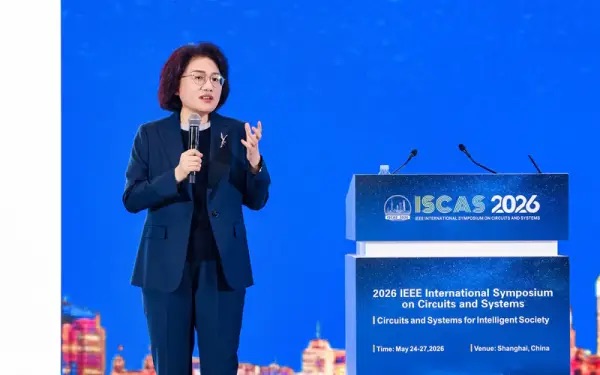
At the 2026 International Symposium on Circuits and Systems (ISCAS 2026) held in Shanghai, Huawei Director and President of its Semiconductor Division, He Tingbo, delivered a keynote speech titled “Semiconductor New Path Exploration and Practice,” officially introducing the Tau (τ) Scaling Law.
This announcement has quickly captured global attention. Rather than continuing to compete solely on shrinking process nodes, Huawei is proposing a fundamentally new technical roadmap: replacing “geometric miniaturization” with “temporal miniaturization” to achieve performance leaps through system-level optimization.
Beyond Moore’s Law: A New Paradigm
For over five decades, Moore’s Law has driven the semiconductor industry by relentlessly shrinking transistor sizes to increase density, boost performance, and reduce power consumption. However, as process technology approaches 2nm and below, physical limits, soaring costs, and yield challenges have become increasingly severe.
Huawei’s Tau (τ) Scaling Law directly addresses this bottleneck. The core idea is to treat the time constant τ (signal propagation delay, where τ = RC, resistance × capacitance) as the new primary metric. The goal is to compress the “travel time” of signals across the entire system, thereby improving overall performance and energy efficiency.
In simple terms:
- Traditional path: Focus on space (smaller transistors).
- Tau path: Focus on time (faster signal transmission).
He Tingbo emphasized that this approach does not abandon process advancements but instead builds a full-stack collaborative optimization system spanning devices, circuits, chips, systems, and data centers. The aim is to deliver equivalent or superior performance using mature or less advanced manufacturing processes.
Core Technology: LogicFolding
The flagship implementation of the Tau Scaling Law is LogicFolding.
Conventional chip designs lay circuits flat on a two-dimensional plane, forcing signals to travel long horizontal distances, which increases latency and power consumption. LogicFolding vertically stacks circuits into multiple layers, replacing long horizontal interconnects with much shorter vertical ones.
According to Huawei:
- On the same process node, LogicFolding significantly improves transistor density, energy efficiency, and operating frequency.
- The upcoming Kirin 2026 chipset will be the first consumer-grade product to fully adopt this technology, scheduled for release in autumn 2026.
- Compared to traditional 2D designs, LogicFolding reportedly increases transistor density by 53.5%, reaching approximately 238 MTr/mm² — performance that approaches or matches leading 3nm-class technologies.
Huawei noted that over the past six years, it has designed and mass-produced 381 chips based on this philosophy, covering smartphones, AI computing, automotive, base stations, and other fields. This provides strong engineering validation for the new law.
Tackling AI Data Center Bottlenecks
Another major focus of the Tau Scaling Law is AI data centers.
Today, one of the biggest constraints in AI training and inference is not raw computing power but the enormous cost of data movement — including transmission latency, energy consumption, and interconnect overhead. Huawei proposes solutions such as unified buses, Hi-ONE optical interconnects, and 3D folding to make large-scale chip clusters function more like a single giant chip, dramatically reducing data movement overhead and improving system efficiency.
This aligns with global industry trends, as TSMC, Intel, and Samsung are heavily investing in advanced packaging technologies. Huawei’s contribution lies in elevating these approaches into a cohesive theoretical framework backed by full-stack software-hardware co-optimization.
Roadmap to 2031: Equivalent to 1.4nm
Huawei’s long-term plan outlines that, through progressive implementation of LogicFolding and related technologies, transistor density and frequency will continue to rise. By 2031, high-end chips based on the Tau Scaling Law are expected to achieve performance equivalent to 1.4nm process technology.
It is important to note that “equivalent to 1.4nm” does not mean mastering 1.4nm lithography. Instead, it represents comprehensive performance parity achieved through multi-dimensional system optimization — a pragmatic “change lanes to overtake” strategy.
Global Significance and China’s Semiconductor Breakthrough
Against the backdrop of ongoing technological competition, the release of the Tau Scaling Law carries symbolic importance. It signals that China’s semiconductor industry is transitioning from “following” to “parallel running — and potentially leading — in specific tracks,” emphasizing system-level innovation, ecosystem collaboration, and supply chain resilience.
He Tingbo concluded by stressing that “the future belongs to open collaboration,” inviting global scientists, engineers, and industry partners to jointly advance the industry.
Challenges Ahead
Vertical stacking introduces new complexities in thermal management, yield control, manufacturing difficulty, and ecosystem adaptation. Real-world validation will ultimately depend on products like the Kirin 2026.
Nevertheless, Huawei’s Tau Scaling Law offers a clear, actionable new path for the industry. It serves as a reminder that when one road is blocked, true wisdom lies in discovering and paving a broader alternative route.
In the critical domain of semiconductors — a field that shapes national competitiveness — Chinese enterprises are writing their own technology narrative through concrete action.
lovelycn.com will continue to track the Kirin 2026 launch, further developments of the Tau Scaling Law, and global semiconductor trends. Stay tuned for in-depth coverage.